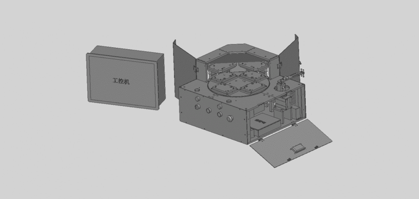
Unlock the world of quality control in electronics with our free technical drawings of a PCB Board Functional Test System. This essential piece of equipment is the final step in a printed circuit board’s journey from production to a final product. The blueprints reveal a complex, automated system designed to simulate the PCB’s operating environment and verify that it performs its intended functions flawlessly. The design showcases the intricate integration of a test jig, precision probes, and a control interface that automates a series of electrical and signal tests, ensuring every board meets strict performance criteria.
This comprehensive drawing package is a must-have resource for engineering students, electronics manufacturers, and anyone interested in the inner workings of automated quality assurance. By studying these plans, you will gain a deeper understanding of the challenges involved in creating a robust and repeatable test environment. The detailed schematics are a perfect educational tool for learning about the principles of test automation, electrical probing, and the importance of fixtures in high-volume production. Download these free, CAD-compatible drawings today to enhance your technical knowledge and streamline your future design projects.
Key Features:
- Test Fixture Design: The drawings detail the “bed-of-nails” test jig, showing how spring-loaded probes make precise contact with test points on the PCB.
- Automated Probing: Blueprints showcase the mechanisms that automate the pressing of the PCB onto the test fixture, ensuring consistent and reliable connections.
- Signal Integration: The plans illustrate how the test system’s probes are connected to a control interface that sends and receives signals to verify functionality.
- Modular and Scalable: The design provides a clear understanding of a system that can be adapted and reconfigured to test different types of PCB boards.